

Select language
The driving force behind our
digital transformation
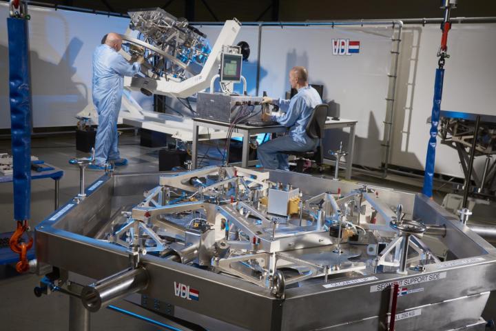
The semiconductor industry is one of the most dynamic and innovative sectors in the world and is also the driving force behind the digital transformation of our society and economy. From smartphones to self-driving cars, artificial intelligence to renewable energy, none of these would be possible without semiconductors. The semiconductor sector is also one of the most competitive and demanding sectors and is propelled by Moore's Law. With the emergence of new theories like 'More Moore' and 'More than Moore' - in which chip architectures are becoming even smaller and more complex, and systems integration is taking off at a tremendous pace – the limits haven't been reached for the moment. On the contrary! There is a constant need for new technologies, materials, and processes to reduce energy consumption and production costs and push the boundaries of what can be achieved. VDL ETG is therefore preparing for further global growth, both in production and design capacity.
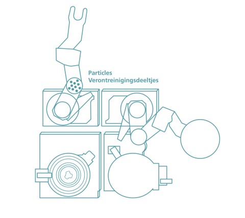
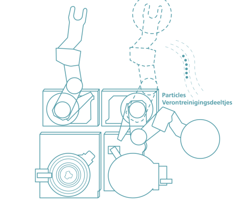
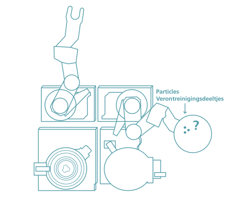
Increasingly stringent cleanliness requirements are proving a major challenge for the industry, however. By investigating how contaminants occur, move, and are deposited, we are finding ways to prevent them ending up in critical locations.

The driving force behind our
digital transformation
The semiconductor industry is one of the most dynamic and innovative sectors in the world and is also the driving force behind the digital transformation of our society and economy. From smartphones to self-driving cars, artificial intelligence to renewable energy, none of these would be possible without semiconductors. VDL ETG is therefore preparing for further global growth, both in production and design capacity.
Increasingly stringent cleanliness requirements are proving a major challenge for the industry, however. By investigating how contaminants occur, move, and are deposited, we are finding ways to prevent them ending up in critical locations.


Global
COOPERATION
The semiconductor industry brings together numerous complex processes and expensive, sophisticated equipment. Many companies supplying this industry are VDL ETG customers. For decades now, we have been working very closely with one of them, a manufacturer of photolithographic equipment, to design and produce modules and systems for their equipment. We are also working with several customers who provide equipment for complex semiconductor processes such as deposition (CVD/PVD), metrology, and inspection.

Tomorrow's
technology
Our involvement extends from the smallest particles on Earth, in CERN's particle accelerator, to the vastness of the universe, with the mirrors of the world's largest telescope in Chile - and everything in between.

Tomorrow's
technology
Our involvement extends from the smallest particles on Earth, in CERN's particle accelerator, to the vastness of the universe, with the mirrors of the world's largest telescope in Chile - and everything in between. Please check the other industries: